Photonicquantum.
Not superconducting circuits in a dilution fridge. Not trapped ions in a vacuum chamber. Light, squeezed through silicon nitride waveguides on a chip you can manufacture today.
Not superconducting circuits in a dilution fridge. Not trapped ions in a vacuum chamber. Light, squeezed through silicon nitride waveguides on a chip you can manufacture today.
The dominant approach to photonic quantum computing uses GKP states. GKP states require on-chip squeezing above 10 dB. No integrated photonic platform has ever demonstrated this. The best published result on-chip is around 8 dB, in a bespoke lab setup, not a manufacturable process.
This is not a minor engineering gap. It is a fundamental manufacturing barrier. Every dB of squeezing demands exponentially better loss control. Integrated photonics has hard physical limits on propagation loss that make 10+ dB a possibly unreachable target on a production line.
We chose a different architecture entirely.
Published academic groups. Commercial SiN foundry process. The physics works today.
The H-cat architecture (Lee, Park, Jeong, PRX Quantum 2024) encodes quantum information in superpositions of coherent states. Cat states are more resilient to the dominant error channel in photonics: photon loss. When a photon is lost, the loss is detectable. Detected errors can be erased rather than corrected.
Spontaneous four-wave mixing in SiN microrings generates squeezed vacuum at telecom wavelengths.
Heralded photon subtraction converts squeezed states into small cat states. Iterative breeding grows amplitude.
Entangling measurements between cat-state qubits implement universal gates without direct interaction.
Photon-number-resolving detectors flag lost photons. The error becomes an erasure, not a mystery.
Surface code with erasure-aware decoding. Loss tolerance an order of magnitude above standard approaches.
The critical insight: loss detection converts quantum errors from invisible corruptions into known erasures. Erasures are exponentially easier to correct. This is why our architecture tolerates physical loss rates that would be fatal in other approaches.
Every component in this pipeline maps to a known photonic device. Microrings for squeezing. Beam splitters for interference. Transition-edge sensors for photon counting. The architecture does not require any device that has not been independently demonstrated. It requires them to work together on one chip.
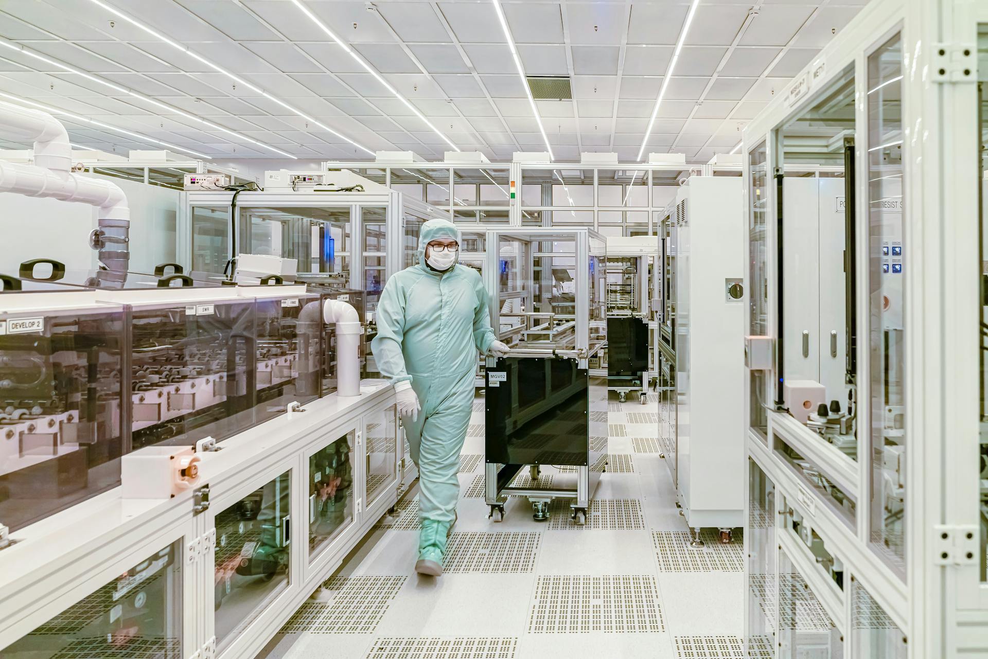
Mature CMOS-compatible platform. Not a hypothetical future fab.
We are not designing for a hypothetical future fabrication process. Our photonic source is built on silicon nitride, a mature, low-loss, CMOS-compatible material system available through established commercial foundry processes.
The device requirements are bounded and achievable. High-Q microring operation requires low propagation loss, a parameter that state-of-the-art SiN processes already satisfy by a comfortable margin. Dispersion engineering identifies the geometry for efficient four-wave mixing at telecom wavelengths.
A hardware validation plan maps each simulation prediction to a physical test structure with quantitative acceptance criteria. This is the plan that converts "simulated" into "measured."
Our required squeezing level has been demonstrated by published academic groups using commercial SiN foundry processes. We do not need a breakthrough. We need integration.
Each generation's overhead is derived from validated simulation parameters. Gen 1 and 2 count NISQ and error-detected qubits. Gen 3 and 4 count fault-tolerant logical qubits. Crossing into true fault tolerance carries a real overhead cost, then scales from there.
Research partnerships. Investment. Joining the team.
Get in Touch